ALD and ALE go Quantum — Research grant for scalable atomic scale processing (ASP) techniques for quantum computing
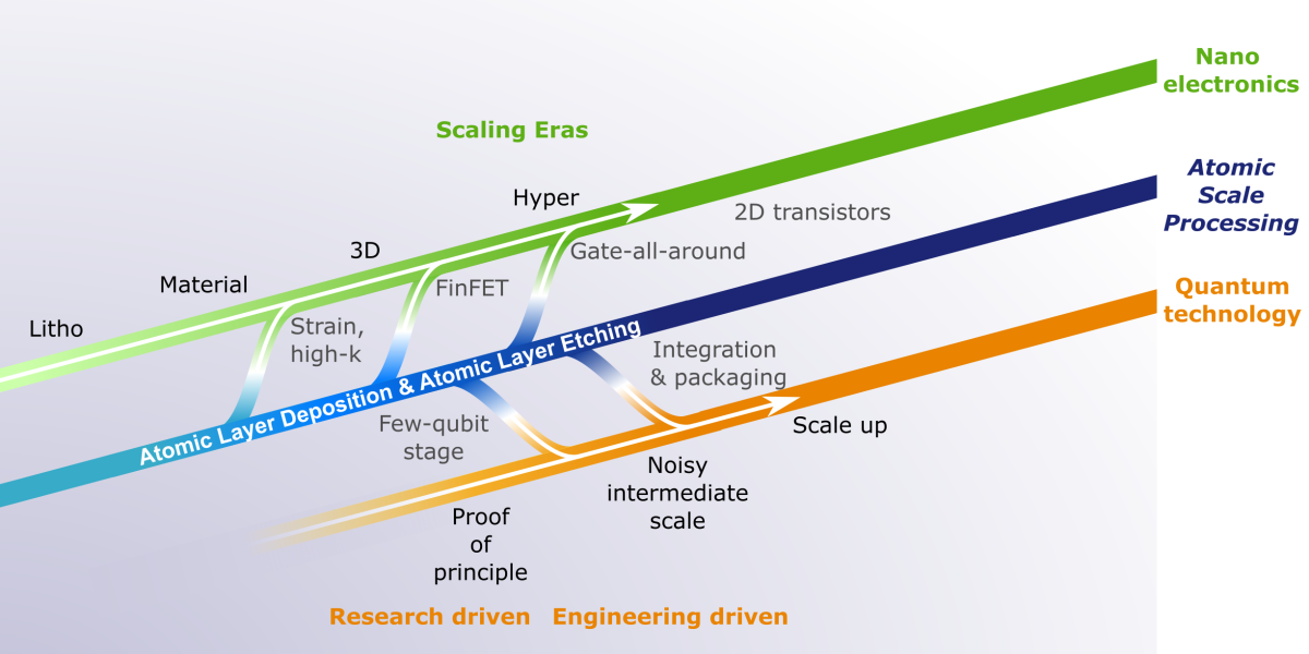
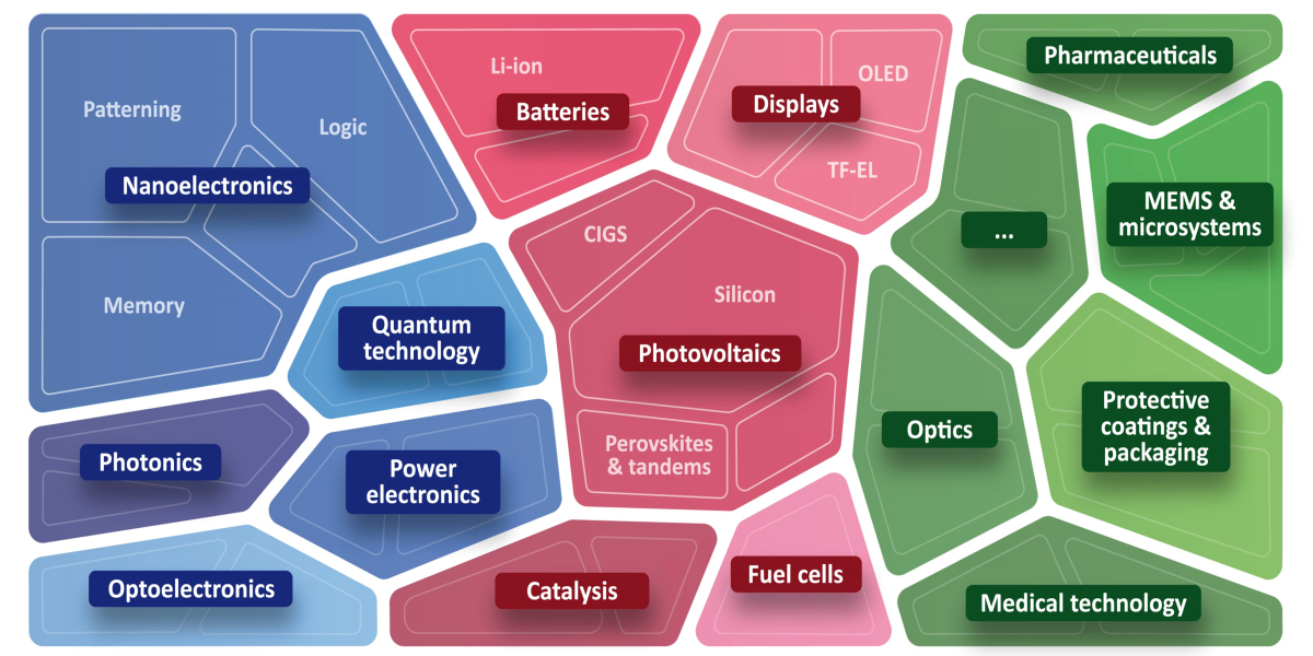
Recently, the Dutch Research Council (NWO) revealed six research projects to receive funding within its Open Technology Programme. We are proud to announce that our project – Atomic Layer Deposition and Etching for Quantum Computing – is among these projects! In this blog we will outline why this project was conceived, and why the addition … Read more
Update of the Atomic Scale Processing ReviewBase – Easy-to-access overview of ALD and ALE reviews (extended), ASD reviews (new) and ALD book chapters (new)

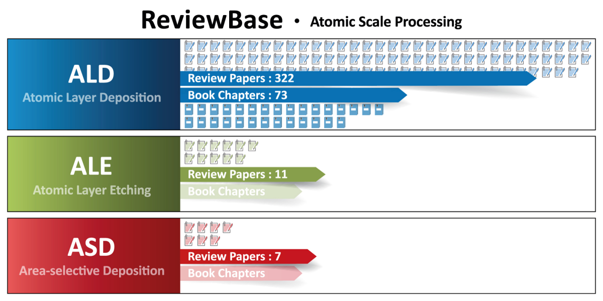
In late March, we launched our ReviewBase, a listing of atomic layer deposition (ALD) and atomic layer etching (ALE) review articles. The ReviewBase files available in Excel and PDF formats have been downloaded more than 500 times altogether in a little over two months. As the AtomicLimits site values open access to information, the ReviewBase … Read more

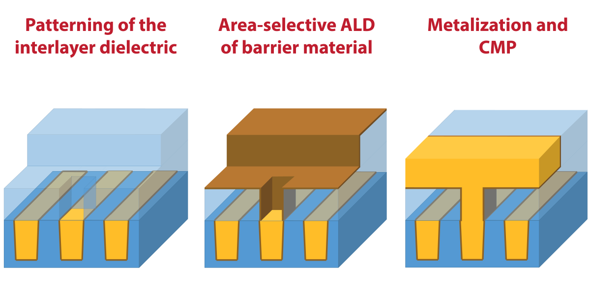
Area-selective ALD of diffusion barriers for via optimization – There is plenty of room at the bottom

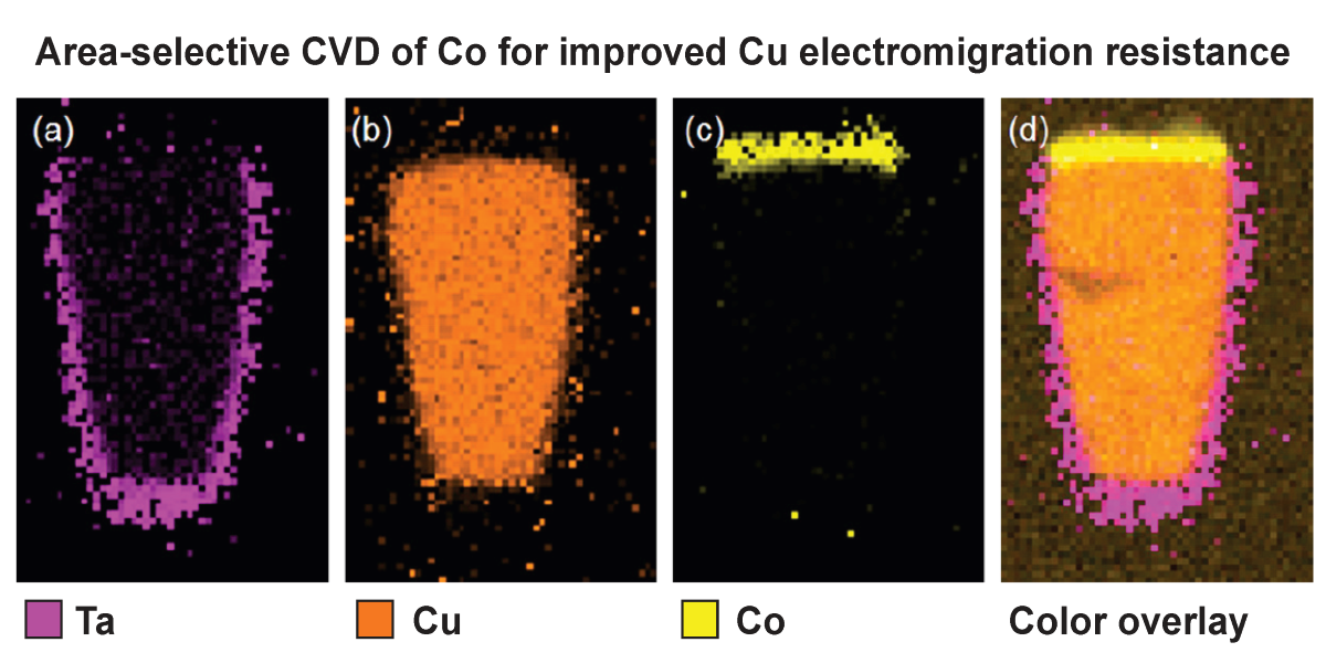
Please cite as M.J.M. Merkx, A.J.M. Mackus, Area-selective ALD of diffusion barriers for via optimization – There is plenty of room at the bottom. 2022, 7. AtomicLimits. This week the 6th area-selective deposition (ASD) workshop will be held in San Francisco, California. During this workshop, we will present our latest work on area-selective ALD of TaN.1 … Read more

Spatial ALD day – June 9th, register here!

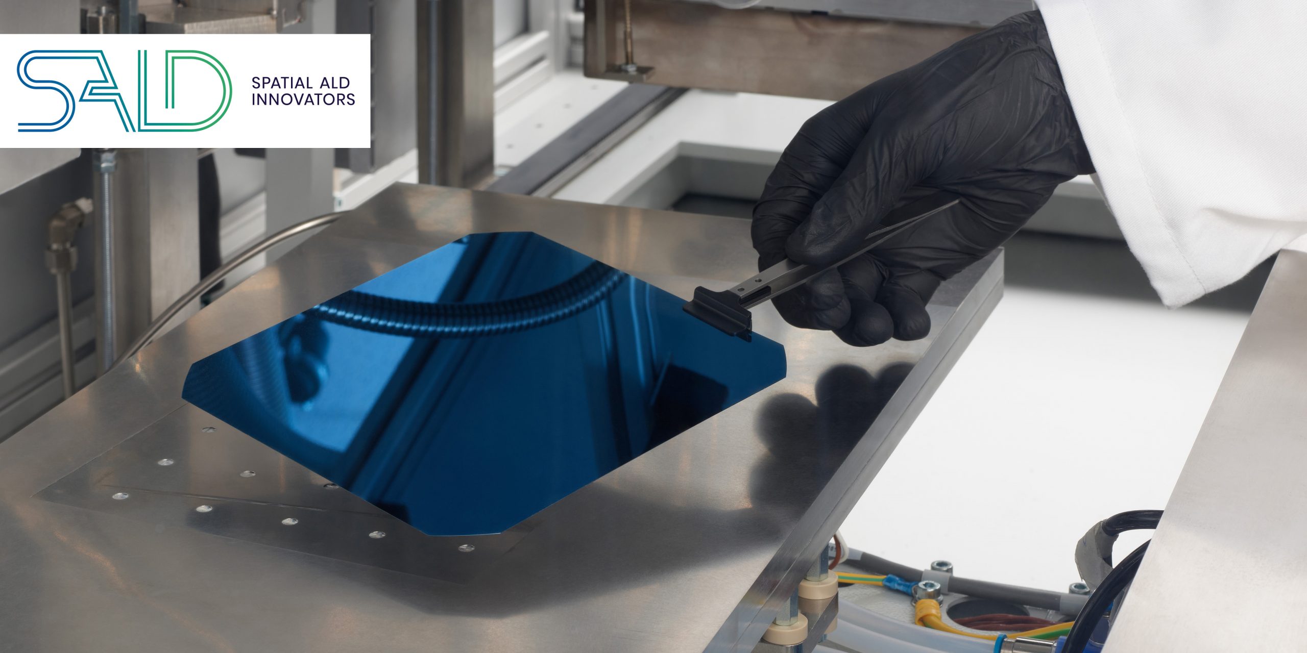
On June 9th 2022, we will organize a spatial ALD day at the Eindhoven University of Technology. This full-day on-site (not online!) event will cover various aspects of spatial ALD, including presentations by spatial ALD companies in the Netherlands, as well as overview and in-depth presentations about (spatial) ALD and its applications. This day is … Read more

Launch of the ALD & ALE ReviewBase – An easy-to-access overview of all ALD and ALE review papers

The scientific and technological interest in atomic layer deposition (ALD) and atomic layer etching (ALE) has been surging in the last decade and the sheer volume of ALD and ALE papers can make it difficult to get a clear overview of what is going on. Luckily, the studies and trends are often summarized and compared … Read more

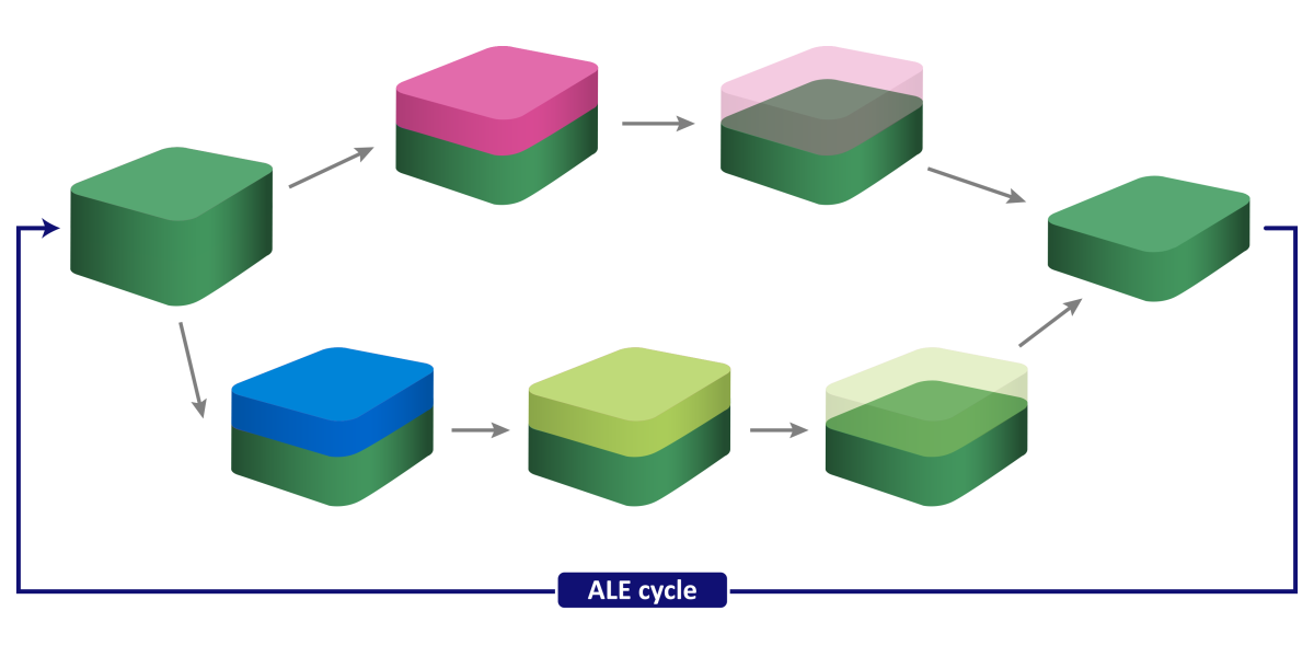
Atomic Layer Etch Carves the Path to More Efficient Computing

Abstract High-volume manufacturing (HVM) of atomic-scale semiconductor devices requires new approaches to deposit and etch materials in complex nano-architectures. Next-generation logic devices, including gate all-around (GAA) transistors and the conductors that link them together, must be engineered with atomic precision. The selective removal of materials also enables efficient integration schemes which mitigate costly lithography issues … Read more

About (my way of) academic leadership
— A reflection after 10 years of chairing the Plasma & Materials Processing group at TU/e

In 2021 it was 10 years ago that I took over the chair position of the Plasma & Materials Processing (PMP) group at the Department of Applied Physics of the Eindhoven University of Technology (TU/e). Since then I have been leading this research group and I thought that it was a good time now to … Read more

X