Passivating Contacts for Silicon Solar Cells — A Zinc Oxide Breakthrough?
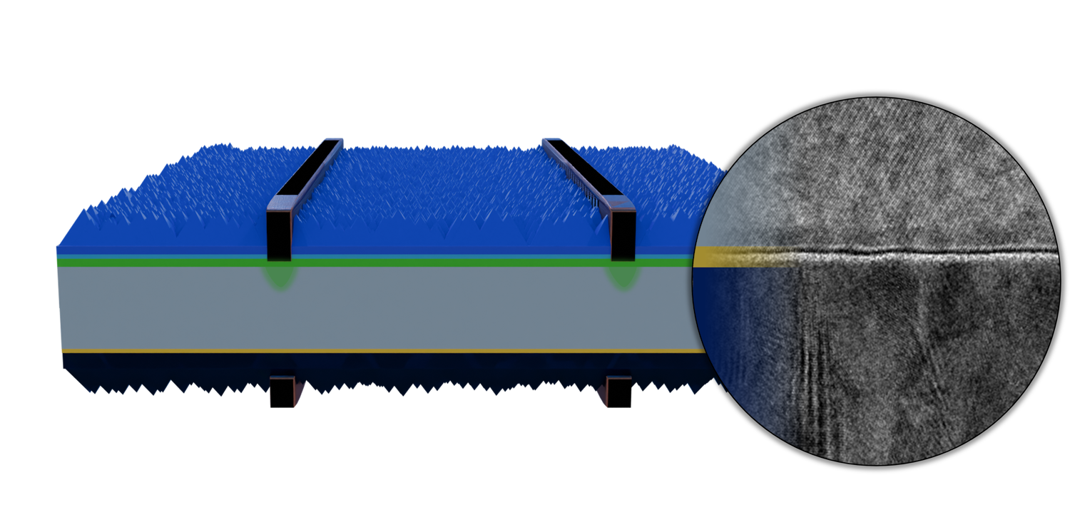
In the field of silicon solar cells, the search for more efficient and cost-effective technologies never ceases. One of the most exciting developments of the past decade has been the rise of so-called passivating contacts, with the current industry leader being TOPCon (Tunnel Oxide Passivated Contact) cells. I remember I was a PhD student when … Read more
ALD and ALE go Quantum — Research grant for scalable atomic scale processing (ASP) techniques for quantum computing

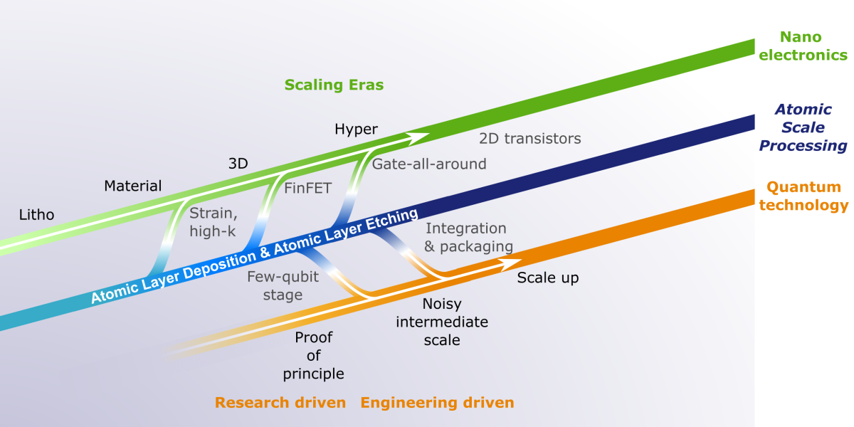
Recently, the Dutch Research Council (NWO) revealed six research projects to receive funding within its Open Technology Programme. We are proud to announce that our project – Atomic Layer Deposition and Etching for Quantum Computing – is among these projects! In this blog we will outline why this project was conceived, and why the addition … Read more

Fully self-aligned vias: the killer application for area-selective ALD? – A discussion of the requirements for implementation in high volume manufacturing

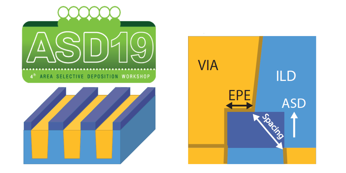
Please cite as: A.J.M. Mackus, M.J.M. Merkx. Fully Self-Aligned Vias: The Killer Application for Area-Selective ALD? – A Discussion of the Requirements for Implementation in High Volume Manufacturing. 2019, 7. AtomicLimits. Recently, the 4th Area Selective Deposition workshop (ASD2019) took place at IMEC in Leuven, Belgium. During this workshop it became clear that the main … Read more

The dawn of atomic-scale processing
– The growing importance of atomic layer deposition and etching

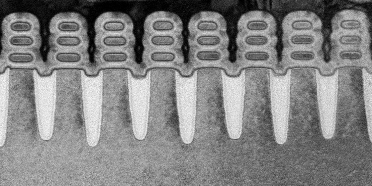
A few weeks ago, the big news was that the research alliance of IBM, Global Foundries and Samsung unveiled the world’s first 5 nm chip as we could all read everywhere over the internet [1]. Most notable was however the fact that they reported the use of horizontal gate-all-around field-effect-transistors (GAA-FETs) in which they actually … Read more

X