

The continued evolution of semiconductor technology—as well as advances in emerging material platforms—places increasingly stringent demands on nanofabrication steps such as etching and deposition. Processes must not only enable atomic-scale thickness control, but also precise control over how surfaces are
Celebrating ALE at ALD/ALE 2025 in Jeju, Korea – Updates to the history, new animations, and insights from industry
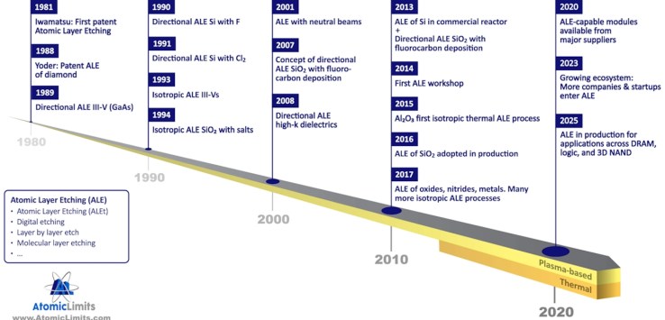
At the end of June (June 22–25, 2025), the ALD/ALE 2025 conference took place in Jeju, South Korea. The conference combines the International Conference on Atomic Layer Deposition (25th edition this year) with the Atomic Layer Etching Workshop (12th edition).

Company Course on Plasma Physics – Teaching Elementary Plasma Physics to Companies in the Eindhoven Brainport Region
Earlier, I wrote a blog post about the significance of plasma physics in EUV lithography and how ASML recognizes its importance—so much that ASML has a portion of their “Research” and “Development & Engineering” staff receive training in elementary plasma

How atomic scale processing can help to pave the way for future quantum devices: A Workshop to bridge ALD/ALE and Quantum communities
As a prelude to our upcoming workshop on atomic layer deposition and etching for quantum technologies, we share our vision in this blog post about how ALD and ALE can help propel quantum technologies forward. Also, a detailed program and

Passivating Contacts for Silicon Solar Cells: A Zinc Oxide Breakthrough?
In the field of silicon solar cells, the search for more efficient and cost-effective technologies never ceases. One of the most exciting developments of the past decade has been the rise of so-called passivating contacts, with the current industry leader

Surface passivation as a cornerstone of modern semiconductor technology – Highlighting a comprehensive review paper on surface passivation for silicon, germanium, and III–V materials
What do transistors, solar cells, microLEDs, and thin-film transistors have in common? At first glance, the answer might seem straightforward: they all rely on semiconductor materials such as silicon (Si), germanium (Ge), gallium arsenide (GaAs), indium phosphide (InP), and gallium

Celebrating the 50th anniversary of ALD at ALD/ALE 2024 in Helsinki! – Updates of the history of ALD in timelines and the animated version of the ALD periodic table
Next week, from August 4 to 7, the ALD/ALE 2024 conference will be held in Helsinki, Finland. This event marks the 24th International Conference on Atomic Layer Deposition and will also include the 11th International Atomic Layer Etching Workshop. This

AI serving the ALD community – Using ChatGPT 4 to extract ALD parameters from scientific papers
Recently, the Plasma and Materials Processing (PMP) group at the TU/e hosted de AI workshop, a company founded by four students that aims to educate and train people about using Artificial Intelligence (AI) for their work, especially ChatGPT 4. The

Introducing the new AtomicLimits ReviewBase – New features, new design and more to come!
We are very excited to announce the release of the totally renewed ReviewBase, which you can find in the menu above. We launched the original ReviewBase in 2022 as an easy-to-access overview of ALD, ALE and ASD review papers and

The Significance of Plasma Physics in EUV Lithography – Teaching ASML employees my Introduction to Plasma Physics course
My main teaching task at the Eindhoven University of Technology takes place in the fall when I teach the MSc course “Physics of Plasmas and Radiation”. This course is mandatory for all our MSc students in Applied Physics that follow