
Advancing Thin Film Metrology in 3D Structures — The Benefits of the PillarHall Concept

This is a blogpost initiated by our sponsor Chipmetrics The rapid advancement of nanoelectronics is driving the transition to 3D vertical scaling, requiring ultra-thin, highly conformal films to be deposited within high-aspect ratio (HAR) structures. As these technological advances push boundaries, precise thin-film metrology becomes paramount. Chipmetrics is leading the charge with its innovative Lateral … Read more
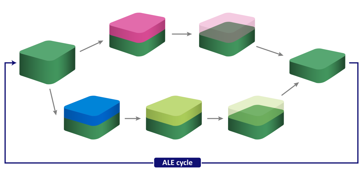
Atomic Layer Etch Carves the Path to More Efficient Computing

Abstract High-volume manufacturing (HVM) of atomic-scale semiconductor devices requires new approaches to deposit and etch materials in complex nano-architectures. Next-generation logic devices, including gate all-around (GAA) transistors and the conductors that link them together, must be engineered with atomic precision. The selective removal of materials also enables efficient integration schemes which mitigate costly lithography issues … Read more

X