ALD/ALE 2026 in Tampa: my Tutorial and AI Everywhere — Slides, live-poll results, and reflections on the current and future perspectives of ALD
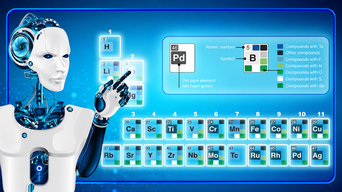
This year, the annual ALD/ALE conference was held in Tampa, Florida (June 28–July 1, 2026). During the tutorial session on Sunday afternoon, I gave a talk titled Current and Future Perspectives on Atomic Layer Deposition. In this blog post, I would like to highlight some of the key messages from that tutorial, along with the … Read more
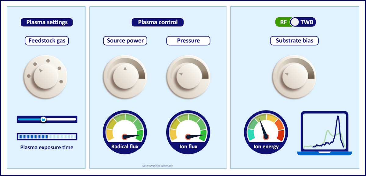
A Closer Look at Tailored Waveform Biasing with an Industrial Generator – New “knobs” for precisely controlling ion energy in ALE and ALD

The continued evolution of semiconductor technology—as well as advances in emerging material platforms—places increasingly stringent demands on nanofabrication steps such as etching and deposition. Processes must not only enable atomic-scale thickness control, but also precise control over how surfaces are modified at the nanoscale. In this context, ion energy is becoming an increasingly important process … Read more

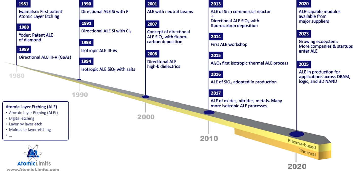
Celebrating ALE at ALD/ALE 2025 in Jeju, Korea – Updates to the history, new animations, and insights from industry

At the end of June (June 22–25, 2025), the ALD/ALE 2025 conference took place in Jeju, South Korea. The conference combines the International Conference on Atomic Layer Deposition (25th edition this year) with the Atomic Layer Etching Workshop (12th edition). Last year we celebrated the 50th anniversary of ALD in Helsinki, and I wrote a … Read more

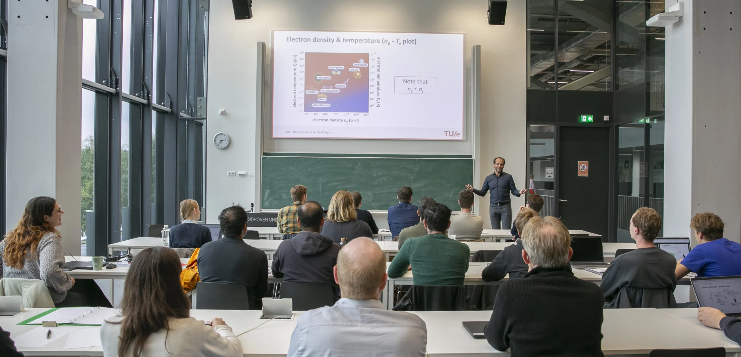
Company Course on Plasma Physics – Teaching Elementary Plasma Physics to Companies in the Eindhoven Brainport Region

Earlier, I wrote a blog post about the significance of plasma physics in EUV lithography and how ASML recognizes its importance—so much that ASML has a portion of their “Research” and “Development & Engineering” staff receive training in elementary plasma physics, in addition to the substantial number of plasma physicists they have directly hired. That … Read more

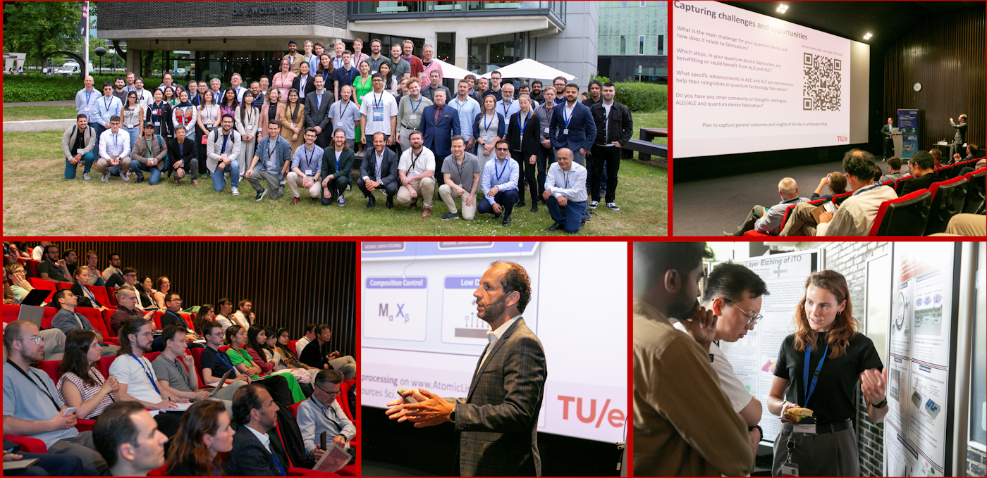
Collaboration at the interface – Takeaways from the ALD/ALE for quantum technologies workshop

On the 20th of May, the atomic layer deposition and etching for quantum technologies workshop took place at the Eindhoven University of Technology. The event was a great success—if we may say so ourselves—and sparked valuable exchanges between the ALD/ALE and quantum communities. In this blog post, we reflect on the day and highlight the … Read more

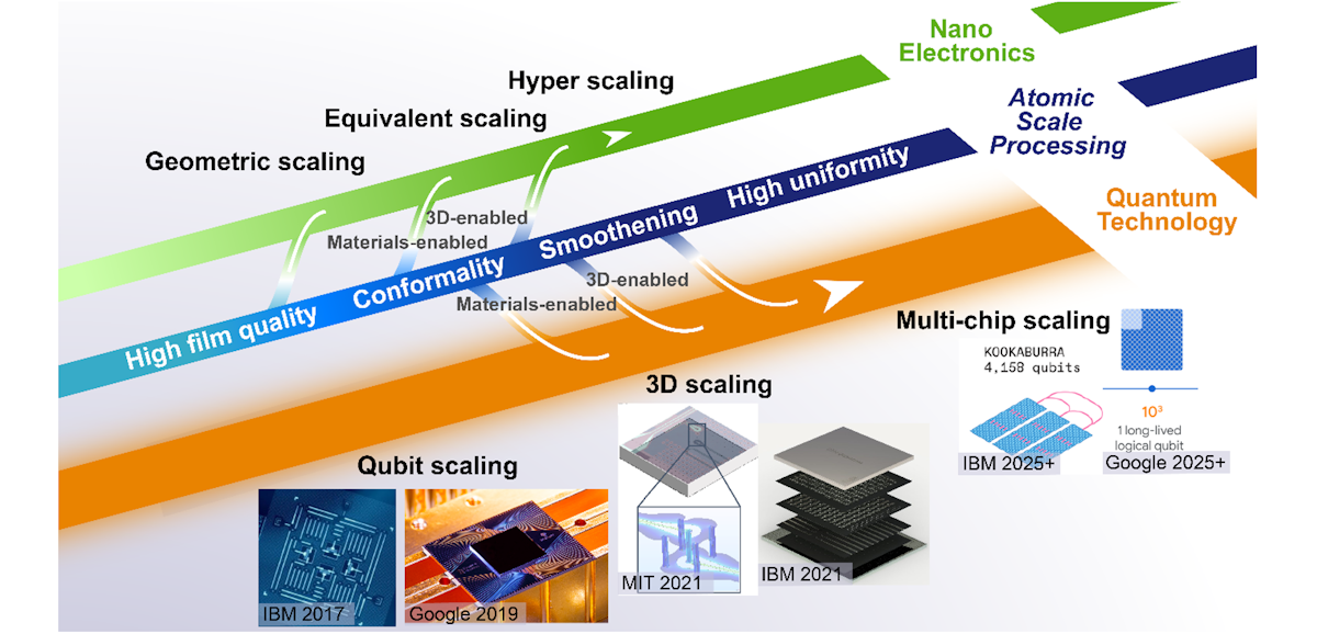
How atomic scale processing can help to pave the way for future quantum devices — A Workshop to bridge ALD/ALE and Quantum communities

As a prelude to our upcoming workshop on atomic layer deposition and etching for quantum technologies, we share our vision in this blog post about how ALD and ALE can help propel quantum technologies forward. Also, a detailed program and the registration link for the workshop are available at the end of this post. We … Read more

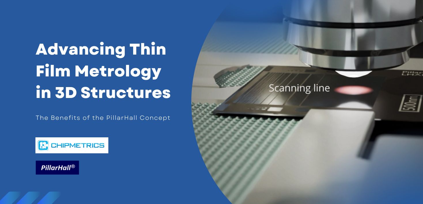
Advancing Thin Film Metrology in 3D Structures — The Benefits of the PillarHall Concept

This is a blogpost initiated by our sponsor Chipmetrics The rapid advancement of nanoelectronics is driving the transition to 3D vertical scaling, requiring ultra-thin, highly conformal films to be deposited within high-aspect ratio (HAR) structures. As these technological advances push boundaries, precise thin-film metrology becomes paramount. Chipmetrics is leading the charge with its innovative Lateral … Read more

X