On February 9, 2022 (1:00 pm – 5:00 pm (EDT) I will give my second AVS Webinar. Last year I gave a webinar about the topic “Plasma-Assisted Atomic Layer Deposition: From Basics to Applications” and this year the topic is again atomic layer deposition (ALD) but now from an application perspective. The latter means that the focus will not lie on explaining the method itself nor on explaining its underlying surface chemistry. The idea is to highlight what one can do with the method. This will still yield a good introduction to the method of ALD and therefore the webinar should be well-suited for newcomers in the field. Yet it should also be very valuable for people interested in thin film technologies and even for experts in the field of ALD because the webinar should give a good overview of where ALD is already used in manufacturing and which applications are at the verge of being introduced industrially.
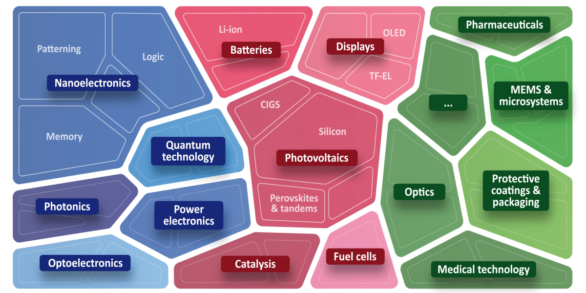
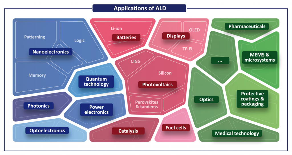
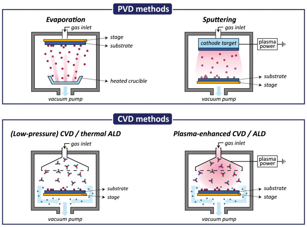
Below you find some of the many images that I’m currently putting together for the webinar. This includes a schematic overview of the application areas of ALD and a schematic that shows how ALD is positioned in the field of vapor phase deposition methods.
A more detailed description of the webinar is given, as well as its objectives, and a link to the registration page. I hope to see many of you online on February 9!
Webinar description
Over the last two decades Atomic Layer Deposition (ALD) has become a key enabling method with a multitude of applications benefiting from the (ultra)thin films that can be prepared with precise thickness control and with unparalleled uniformity and conformality on substrates with a demanding surface topology. In this webinar the method of ALD will be presented with a focus on various applications of ALD: both in the lab and in the fab; from high volume manufacturing to niche markets; from emerging technologies to proof-of-concepts. Special attention will be given to the key features that ALD provides for these specific applications as well as the associated ALD configurations and types of equipment. Application fields that will be addressed include logic and memory devices; advanced patterning applications; power electronics; sensors and detectors; micro-electromechanical systems (MEMS); optics and photonics; photovoltaics; displays; encapsulation and surface engineering technologies; optical, decorative, biomedical, anti-corrosion, and other protective coatings; catalysis and electrochemistry; quantum technology, etc.
Webinar objectives
- Present the basic concepts of ALD and its various configurations
- Provide an overview of ALD materials and types of ALD equipment
- Present applications of ALD in the semiconductor industry, including in logic, memory and patterning
- Give an insight into applications of ALD in other (emerging) high volume manufacturing markets including photovoltaics, battery technology, displays, etc.
- Discuss many other applications of ALD in niche markets and in research labs: from protective to optical coatings and from biomedical applications to catalysis and quantum technology