

Atomic Layer Etch Carves the Path to More Efficient Computing
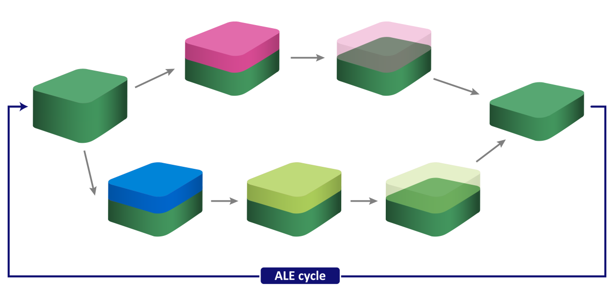
Abstract High-volume manufacturing (HVM) of atomic-scale semiconductor devices requires new approaches to deposit and etch materials in complex nano-architectures. Next-generation logic devices, including gate all-around (GAA) transistors and the conductors that link them together, must be engineered with atomic precision. The selective removal of materials also enables efficient integration schemes which mitigate costly lithography issues … Read more