
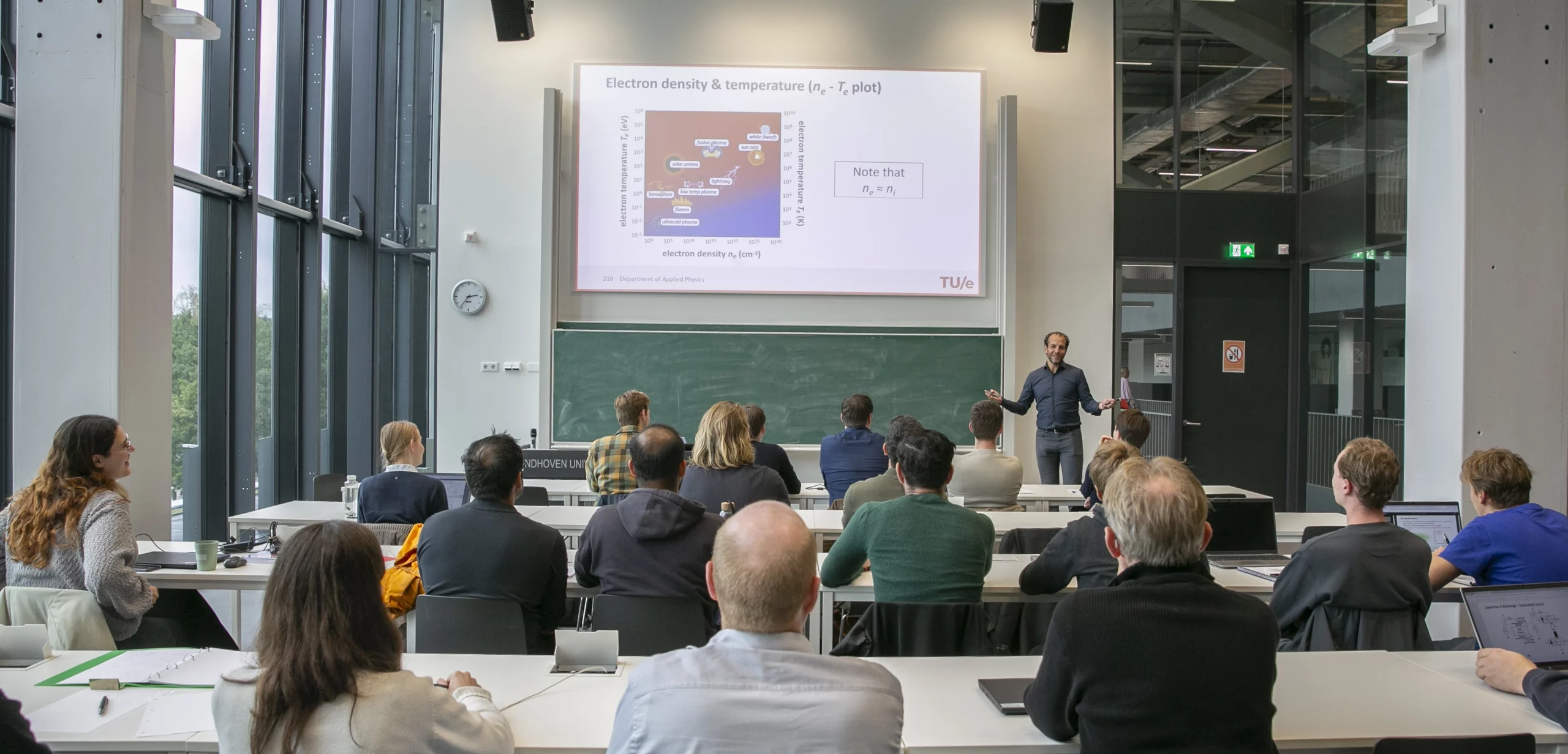
Earlier, I wrote a blog post about the significance of plasma physics in EUV lithography and how ASML recognizes its importance—so much that ASML has a portion of their “Research” and “Development & Engineering” staff receive training in elementary plasma physics, in addition to the substantial number of plasma physicists they have directly hired. That post was inspired by a company course I taught to ASML employees in 2023.
This new post is about the follow-up course I taught last year (September–October 2024), again to ASML employees, but this time also to employees from other companies based mainly in the Eindhoven Brainport region. For readers unfamiliar with the term Brainport: it’s a play on “seaport” and “airport,” referring to a hub for innovation and high-tech industry—here in the Eindhoven area, the focus is on technology and knowledge rather than ships or planes.
Yes, I’m a bit late publishing this (given that the course wrapped up last year), but I have two good reasons for writing now. First, I’d like to share additional insights about the course, its contents, and—importantly—why companies outside ASML are also interested in plasma physics. Second, I’ll be running the course again soon, starting the first week of September, and this post might help potential participants decide to join. There’s still time to register—just get in touch with me directly. Please note: this will be an in-person course at my university, the Eindhoven University of Technology (TU/e). An online version may be considered later.
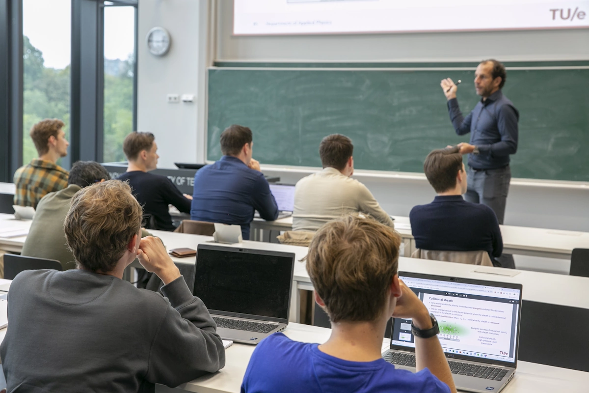
Photo Odette Beekmans (Photodette)
Looking Back at Last Year’s Course
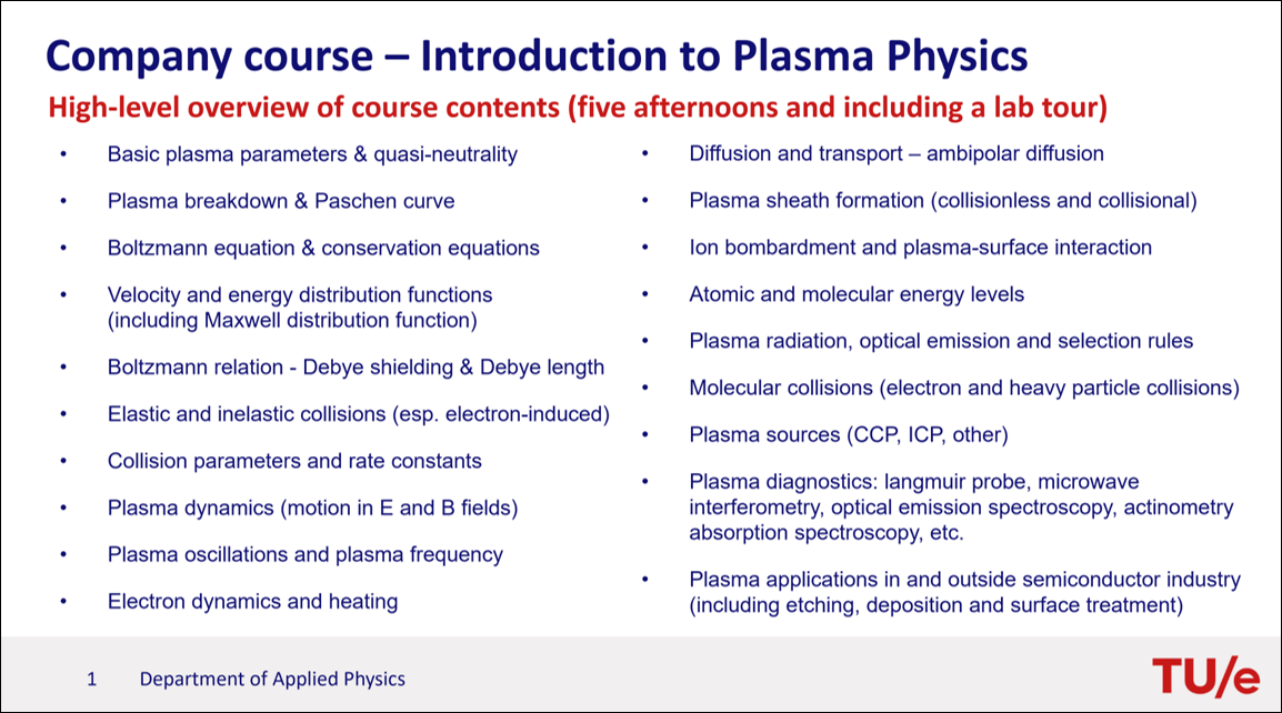
The 2024 edition followed essentially the same program as in 2023, which is based on the MSc course “Physics of Plasmas and Radiation” that I teach to Applied Physics students in the “Plasma & Beams” track. You can find more details in my earlier blog, but for reference, the main subjects of the course are summarized on the slide below.
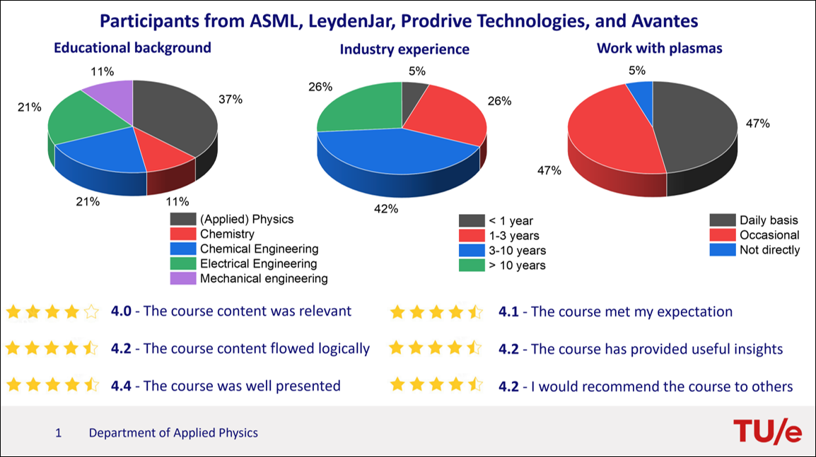
We had 40 participants in total. ASML employees made up the majority, but just under half came from other companies: LeydenJar, Prodrive Technologies, and Avantes. I’m jumping ahead a little here, but I can already say that the feedback from participants was again very positive, as shown in the end-of-course questionnaire results (see below).
ASML’s Perspective
In my previous blog, I explained why ASML values plasma physics training for their staff. Let me add one more telling anecdote. Last year in April, just days after taking over as CEO from Peter Wennink, Christophe Fouquet visited our university. Alongside TU/e’s leadership and some of our students, I joined in welcoming him with presentations and a tour of our NanoLab cleanroom and other labs.
Some of my students showcased their plasma physics and semiconductor research. Christophe’s remark was memorable: understanding plasma physics is extremely important for ASML. Given the complexity of EUV lithography systems, ASML faces many engineering challenges, he said, but controlling the EUV-induced plasma and its interaction with surfaces is their most difficult and important challenge. That statement alone underscores the relevance of the course.
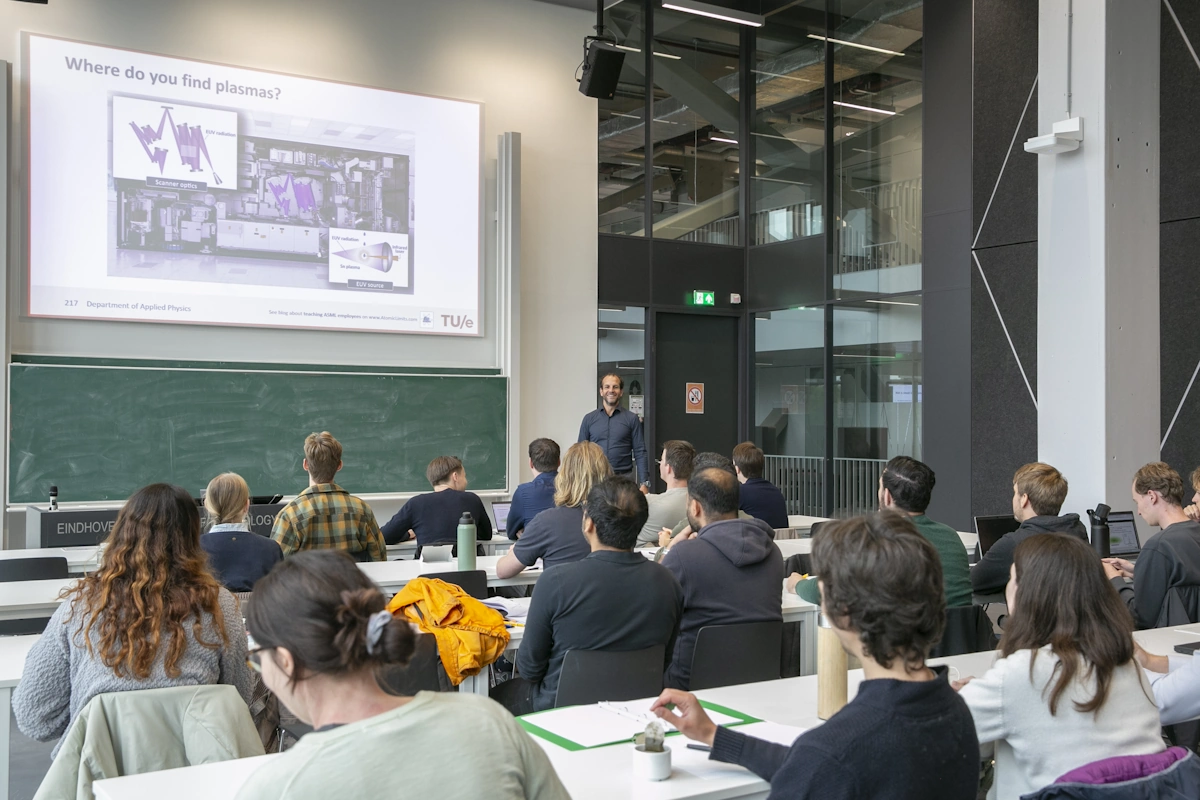
Photo Odette Beekmans (Photodette)
LeydenJar
LeydenJar contributed the second-largest group of participants. The company’s name is a nod to the Leyden jar, one of the earliest devices for storing electric charge, invented in the 18th century in the Dutch city of Leiden—where one of the company’s R&D labs is located.
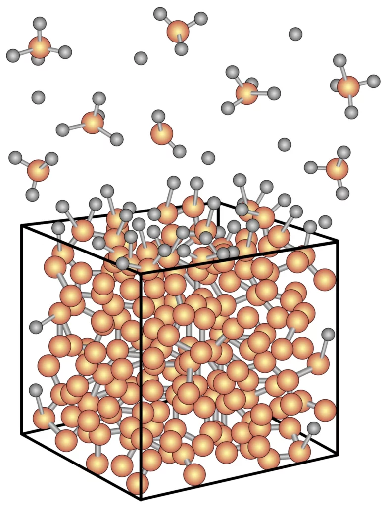
LeydenJar is developing next-generation lithium-ion battery technology by replacing conventional graphite anodes with 100% silicon anodes. Silicon can host roughly ten times more lithium ions than graphite, enabling much thinner anodes while boosting battery energy density. Their production facility in Eindhoven uses plasma-enhanced chemical vapor deposition (PECVD) in a roll-to-roll process to deposit amorphous silicon on copper foil.
Optimizing such a process requires more than just knowing how to operate the tool—you need to understand the underlying plasma physics and plasma chemistry. This is where the course comes in. (I’ve previously reported on a similar PECVD approach by another company)
Prodrive Technologies
Several employees from Prodrive Technologies also attended. Based in Eindhoven and founded by TU/e alumni, Prodrive is a technology-driven company that develops and manufactures electronics, embedded software, and mechatronic systems for a wide range of industries—including semiconductor equipment (ASML is one of their major customers), medical devices, and automotive.
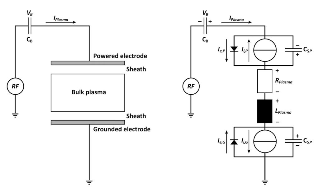
Our group has collaborated with Prodrive for many years, particularly on power supplies for plasma equipment in the semiconductor industry. One highlight is a commercial power supply for tailored waveform biasing—a technique we began researching 20 years ago, now seeing industrial adoption. This tailored waveform generator is making its way into semiconductor fabs, and we have also started collaborating with them on another class of plasma power supplies. Their engineers benefit from understanding plasma reactors not just from a physical perspective, but also as equivalent electrical circuits, which is a topic covered in the course.
Avantes
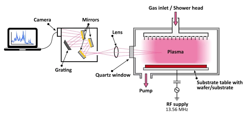
Avantes is a Dutch company specializing in fiber-optic spectroscopy solutions, including light sources, spectrometers, and accessories for scientific and industrial applications. Their systems are used worldwide for chemical and material analysis, quality control, environmental monitoring—and, importantly for this discussion, plasma diagnostics. One key technique is optical emission spectroscopy (OES), which measures the light emitted by excited species in a plasma to infer properties such as plasma composition, electron temperature, or plasma uniformity, etc.
For Avantes engineers, a solid grounding in plasma physics helps in two major ways: it improves their ability to interpret measurement data accurately, and it enables them to better understand and anticipate the needs of customers who work with plasmas daily.
Why It Matters for Eindhoven Brainport Companies
Hopefully this gives you a clearer picture of why companies in the Eindhoven Brainport region—not just semiconductor giants like ASML—value plasma physics expertise. From EUV lithography to battery manufacturing, from plasma power supply engineering to optical diagnostics, plasmas play an important role in many enabling technologies. With several plasma research groups (including our Plasma & Materials Processing group), TU/e is fortunate to have this expertise in-house, and I’m always happy to see it being shared with industry through courses like this.
With so many companies in the region working directly or indirectly on plasma-related technology, I hope to welcome even more participants—whether this year or in future editions. If your work touches on plasmas, this course can help you understand them more deeply, talk about them more confidently, and maybe even solve problems you didn’t realize were plasma-related.
I would like to thank Prof. Richard Engeln and Dr. Seth Brussaard of ASML again for taking the initiative for the course, in 2024 but also in 2025.
