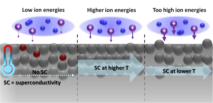
Substrate biasing as a tuning knob for superconducting films – the “ALD and ALE for quantum project” celebrates its first year with a publication

In July 2022 we announced the research grant for the ‘Atomic Layer Deposition and Etching for Quantum Computing’ NWO project on AtomicLimits. This project focusing on atomic scale processing for superconducting quantum devices had a flying start in October 2022. One year later we can look back at a productive first year. It was a … Read more

After enabling AI it is time for the plasma community to benefit from AI – Personal view in a short perspective article

This blog post is about a short perspective article that I recently wrote for the ILTPC newsletter. ILTPC stands for the International Low Temperature Plasma Community. It is one of the two main communities where I feel at home. The other one is the atomic scale processing community. This one is basically the atomic layer … Read more

Let’s chat GPC by chatGPT – Putting ChatGPT to the test and a first (?) article about ALD by AI

I’m sure you have heard the buzz in the field of artificial intelligence (AI)… The promise of AI is to augment human abilities in areas such as decision-making, problem-solving, and other tasks. AI systems aim to simulate human intelligence and learn from data to improve their performance over time. ChatGPT is an AI language model … Read more

A review on Atomic Layer Deposition of (semi)conductive oxides – The role of ALD in these emerging materials and their applications

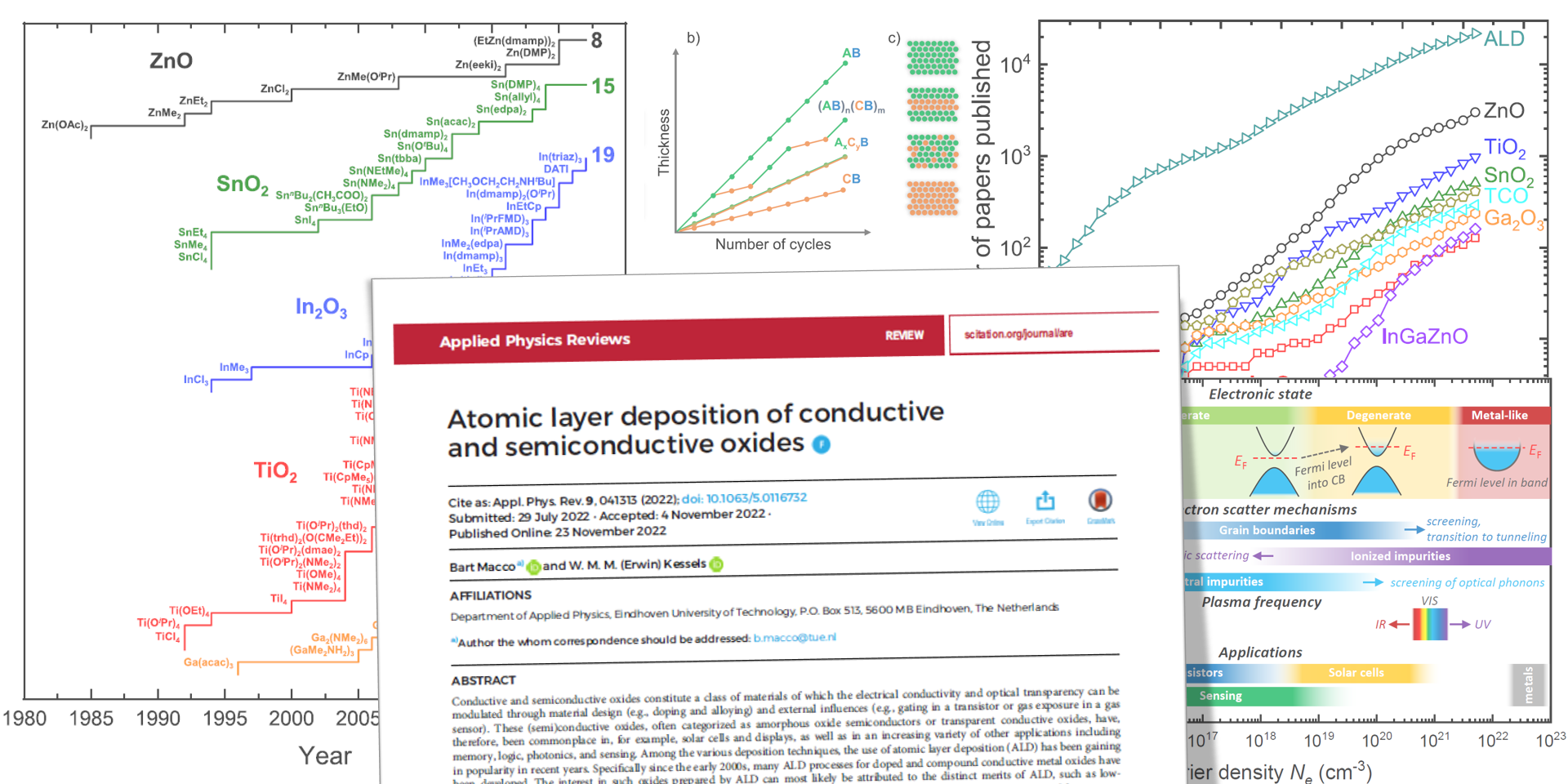
Quick link to open access paper: Applied Physics Reviews 9, 041313 (2022) Earlier this month I published my review paper entitled Atomic layer deposition of conductive and semiconductive oxides. It was an invited review for Applied Physics Reviews and I was very happy to see it picked as Featured article![1] In case you are not familiar … Read more

Foundations of atomic-level plasma processing in nanoelectronics – Smaller, thinner, taller, etc … all enabled by plasmas

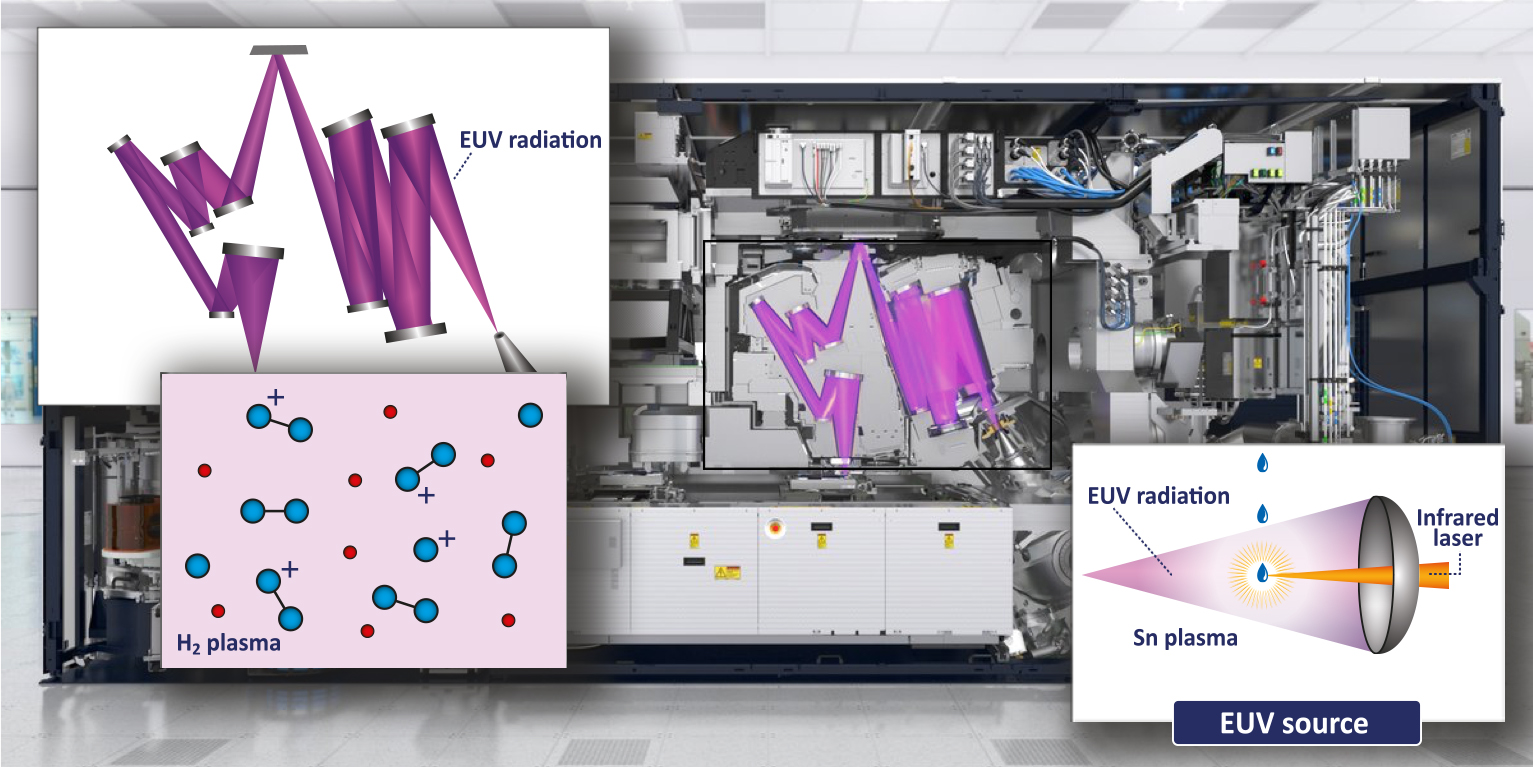
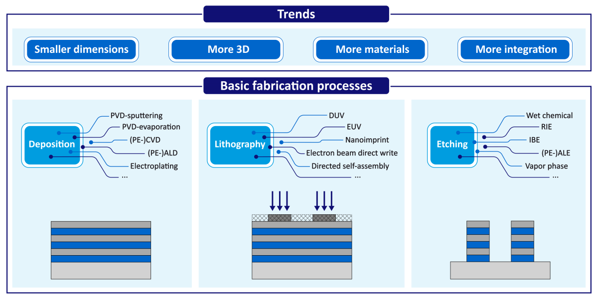
***Quick link to the open access paper: “Foundations of atomic-level plasma processing in nanoelectronics”*** We have just published a topical review paper entitled “Foundations of atomic-level plasma processing in nanoelectronics” in the journal Plasma Sources Science and Technology. This review is part of a two-part collection of papers on Foundations of Low Temperature Plasmas and … Read more

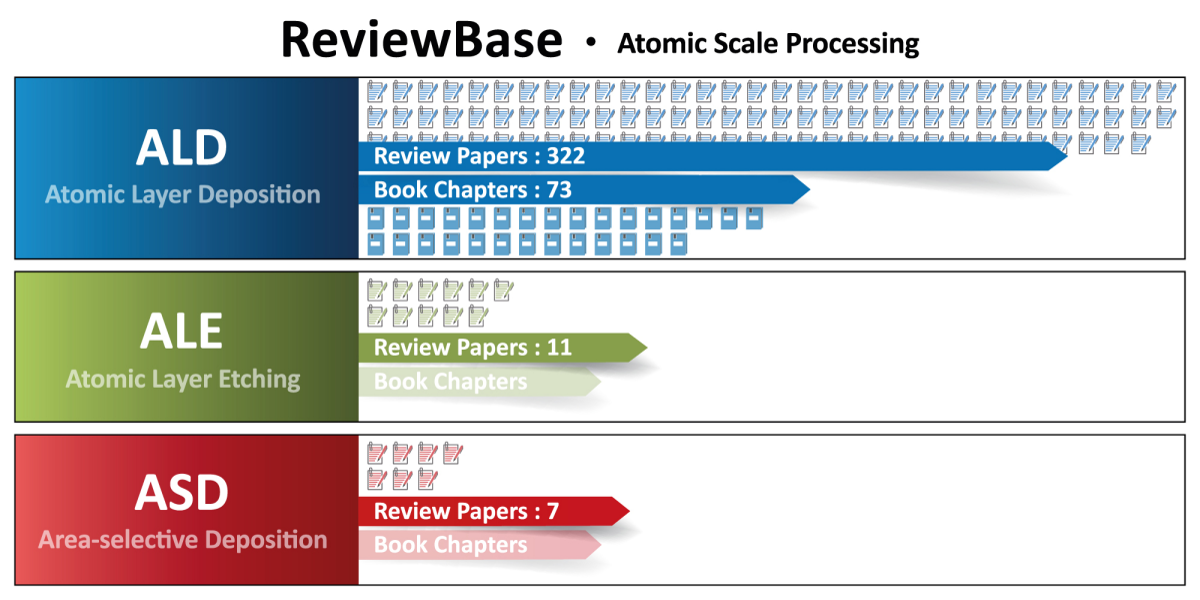
Update of the Atomic Scale Processing ReviewBase – Easy-to-access overview of ALD and ALE reviews (extended), ASD reviews (new) and ALD book chapters (new)

In late March, we launched our ReviewBase, a listing of atomic layer deposition (ALD) and atomic layer etching (ALE) review articles. The ReviewBase files available in Excel and PDF formats have been downloaded more than 500 times altogether in a little over two months. As the AtomicLimits site values open access to information, the ReviewBase … Read more

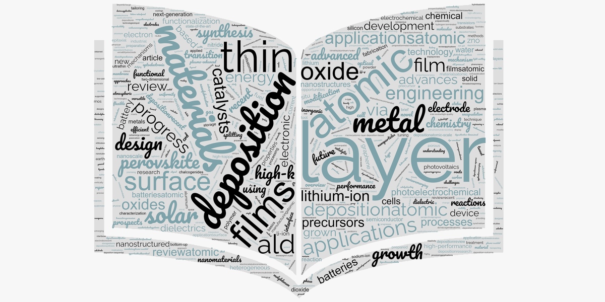
Launch of the ALD & ALE ReviewBase – An easy-to-access overview of all ALD and ALE review papers

The scientific and technological interest in atomic layer deposition (ALD) and atomic layer etching (ALE) has been surging in the last decade and the sheer volume of ALD and ALE papers can make it difficult to get a clear overview of what is going on. Luckily, the studies and trends are often summarized and compared … Read more

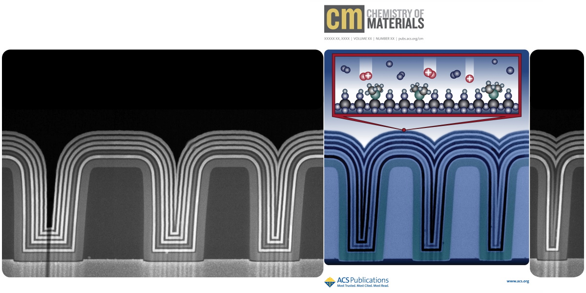
Conformal deposition and gap-fill by plasma ALD – some great TEM images and recently published cover art

The ability of atomic layer deposition (ALD) to grow highly conformal thin films is one of the main reasons why ALD is so popular in research and heavily employed in the semiconductor industry.1,2 This not only holds for thermally-driven ALD. As explained in a previous post, also plasma-assisted ALD can penetrate very deep into high-aspect-ratio … Read more

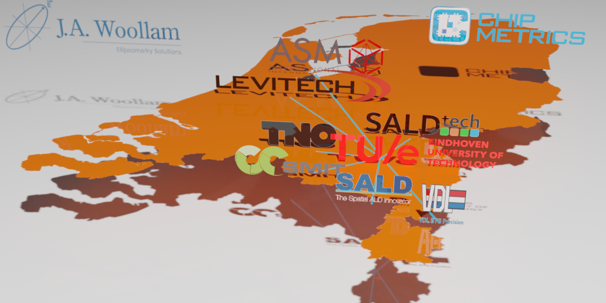
Diving into the Fundamentals of Spatial Atomic Layer Deposition – Strengthening the S-ALD hub in Brainport region Eindhoven

On May 1st, we kicked off our new research project entitled “Spatial Atomic Layer Deposition – More Materials, More Demanding Applications” , granted by the NWO Domain Applied and Engineering Sciences. As the title suggests, the project is geared at making more materials by spatial atomic layer deposition (S-ALD) for more demanding applications, of which … Read more

A new flavor of ALE – What plasmas can bring to isotropic etching (a radical approach)

Plasmas can offer more than just etching straight down. This blog post aims to show that the etching community can benefit greatly from using plasmas for new applications. Currently, in the atomic layer etching (ALE) community plasmas are often considered only for anisotropic etching. In our recent work, which you can read or alternatively watch … Read more

X