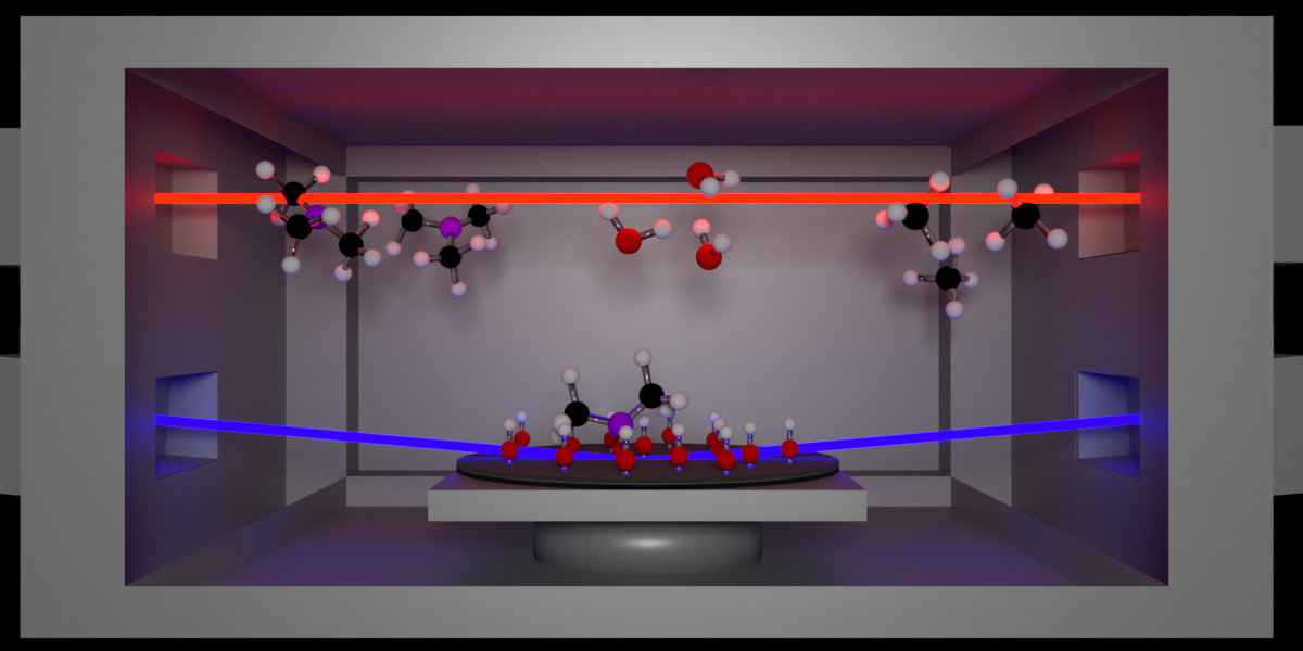
ALD and ALE go Quantum — Research grant for scalable atomic scale processing (ASP) techniques for quantum computing
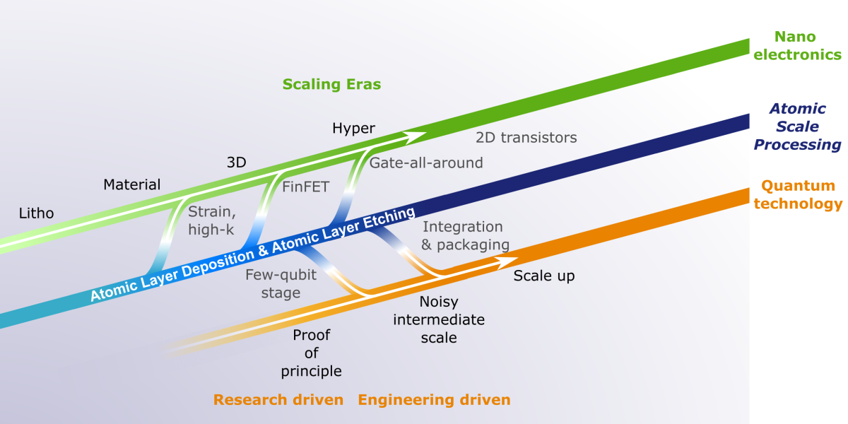
Recently, the Dutch Research Council (NWO) revealed six research projects to receive funding within its Open Technology Programme. We are proud to announce that our project – Atomic Layer Deposition and Etching for Quantum Computing – is among these projects! In this blog we will outline why this project was conceived, and why the addition … Read more
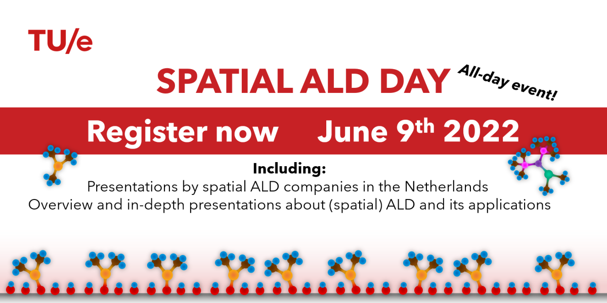
Spatial ALD day – June 9th, register here!

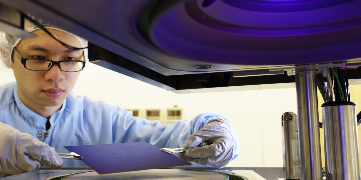
On June 9th 2022, we will organize a spatial ALD day at the Eindhoven University of Technology. This full-day on-site (not online!) event will cover various aspects of spatial ALD, including presentations by spatial ALD companies in the Netherlands, as well as overview and in-depth presentations about (spatial) ALD and its applications. This day is … Read more

Launch of the ALD & ALE ReviewBase – An easy-to-access overview of all ALD and ALE review papers

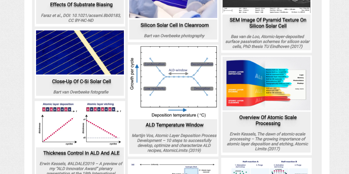
The scientific and technological interest in atomic layer deposition (ALD) and atomic layer etching (ALE) has been surging in the last decade and the sheer volume of ALD and ALE papers can make it difficult to get a clear overview of what is going on. Luckily, the studies and trends are often summarized and compared … Read more

Diving into the Fundamentals of Spatial Atomic Layer Deposition – Strengthening the S-ALD hub in Brainport region Eindhoven

On May 1st, we kicked off our new research project entitled “Spatial Atomic Layer Deposition – More Materials, More Demanding Applications” , granted by the NWO Domain Applied and Engineering Sciences. As the title suggests, the project is geared at making more materials by spatial atomic layer deposition (S-ALD) for more demanding applications, of which … Read more

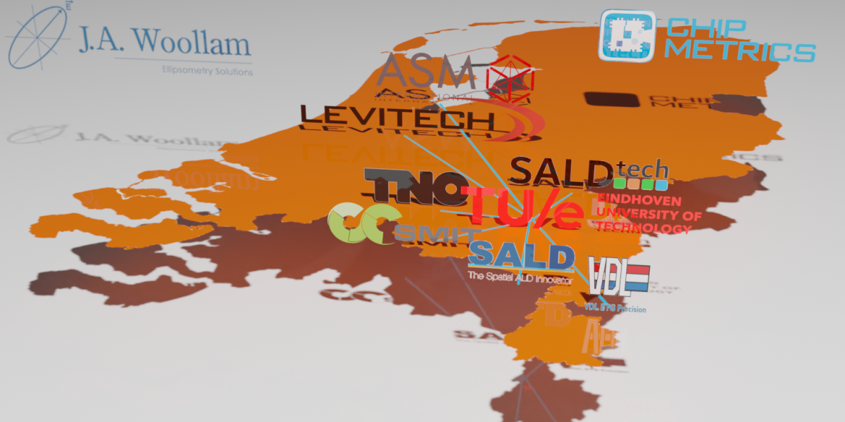
ALD in the Netherlands – Special issue of the NEVAC magazine (free): How a small country can be big in nanolayers

The Dutch Vacuum Society – or Nederlandse Vacuümvereniging (NEVAC) – publishes the so-called “NEVAC blad”, a magazine that appears three times a year. The issue for June 2020 just appeared and it is a special issue completely devoted to atomic layer deposition (ALD). Together with my colleague Bart Macco, I was the guest editor. Originally … Read more

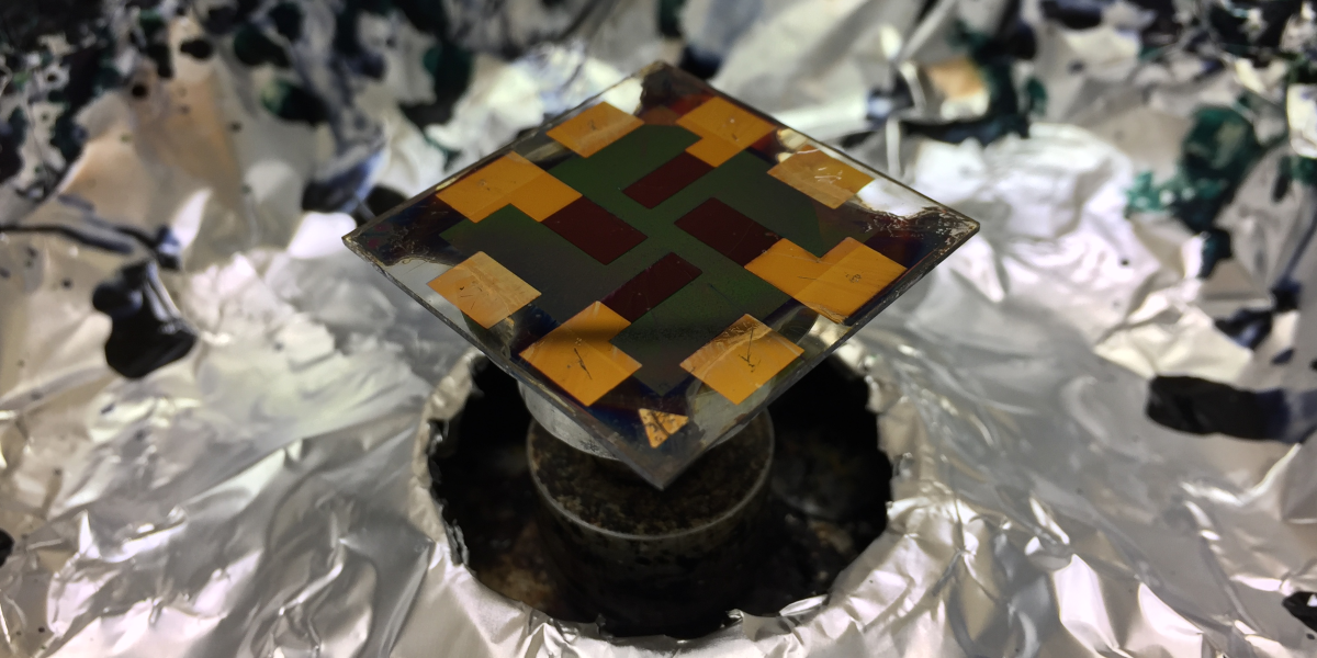
What can Atomic Layer Deposition do for solar cells? – A few afterthoughts from my ALD conference tutorial

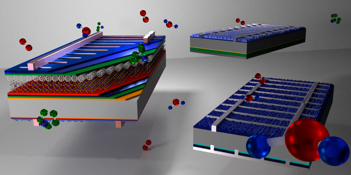
At the end of July the annual AVS International Conference on Atomic Layer Deposition (ALD) – combined with the Atomic Layer Etching (ALE) Workshop – took place in Bellevue, Seattle. As customary, the Sunday before the conference itself was devoted to tutorials, each about 45 minutes long. In previous years the focus was mainly on fundamentals … Read more

In situ Studies of ALD Processes & Reaction Mechanisms

It is the time of the year that the annual AVS International Conference on Atomic Layer Deposition combined with the International Atomic Layer Etching Workshop takes place. The location of 18th edition of the ALD conference (ALD 2018) and the 5th edition of the ALE workshop (ALE 2018) is Incheon, South Korea (July 29 – … Read more

4th Dutch perovskite workshop

Date, time and location of the event The 4th Dutch Perovskite Workshop is scheduled to take place at the Eindhoven University of Technology (TU/e) on Friday 29 June 2018. The program will start at 10:00 hr in the Film Zaal (1st floor) of the Zwarte Doos on the TU/e Campus. Aim and topics The PV … Read more

Advancing PV: from passivation to contacts
– A passivating contact workshop

Aim – The goal of this one-day workshop is to provide a platform to learn more about passivating contacts for crystalline silicon solar cells. Unlike the PV conferences where this topic already receives a fair amount of attention, this platform will enable a more in-depth discussion on the physics of the materials and the related solar … Read more

X