

A little over a month ago, we proudly hosted the second edition of Spatial ALD Day in Eindhoven. After our first edition in 2022, we were thrilled to finally bring the community together again! Spatial ALD Day 2.0 was organized
Register now – Spatial ALD Day 2.0 – October 28, 2025
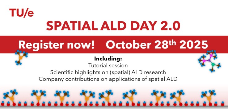
Registration closed Register now for the second edition of the Spatial ALD Day, which will take place on Tuesday, October 28, 2025! This event follows the highly successful first Spatial ALD Day in 2022. Now, we look forward to bringing

Advancing Thin Film Metrology in 3D Structures: The Benefits of the PillarHall Concept
This is a blogpost initiated by our sponsor Chipmetrics The rapid advancement of nanoelectronics is driving the transition to 3D vertical scaling, requiring ultra-thin, highly conformal films to be deposited within high-aspect ratio (HAR) structures. As these technological advances push

Save the Date & Register Now: Second Edition of the Spatial ALD Day – October 28, 2025
We are excited to announce the second edition of the Spatial ALD Day, which will take place on Tuesday, October 28, 2025! This event follows the highly successful first Spatial ALD Day we organized at the start of our NWO

Passivating Contacts for Silicon Solar Cells: A Zinc Oxide Breakthrough?
In the field of silicon solar cells, the search for more efficient and cost-effective technologies never ceases. One of the most exciting developments of the past decade has been the rise of so-called passivating contacts, with the current industry leader

Surface passivation as a cornerstone of modern semiconductor technology – Highlighting a comprehensive review paper on surface passivation for silicon, germanium, and III–V materials
What do transistors, solar cells, microLEDs, and thin-film transistors have in common? At first glance, the answer might seem straightforward: they all rely on semiconductor materials such as silicon (Si), germanium (Ge), gallium arsenide (GaAs), indium phosphide (InP), and gallium

Introducing the new AtomicLimits ReviewBase – New features, new design and more to come!
We are very excited to announce the release of the totally renewed ReviewBase, which you can find in the menu above. We launched the original ReviewBase in 2022 as an easy-to-access overview of ALD, ALE and ASD review papers and

A review on Atomic Layer Deposition of (semi)conductive oxides – The role of ALD in these emerging materials and their applications
Quick link to open access paper: Applied Physics Reviews 9, 041313 (2022) Earlier this month I published my review paper entitled Atomic layer deposition of conductive and semiconductive oxides. It was an invited review for Applied Physics Reviews and I was

Looking back at the Spatial ALD day -with photos and downloadable presentations!
At the start of summer we hosted the first Spatial ALD day at the Eindhoven University of Technology. In this blogpost, I want to look back at this day with a few highlights. Also, you can find photos and downloadable

Spatial ALD day – June 9th, register here!
On June 9th 2022, we will organize a spatial ALD day at the Eindhoven University of Technology. This full-day on-site (not online!) event will cover various aspects of spatial ALD, including presentations by spatial ALD companies in the Netherlands, as