The dawn of atomic-scale processing
– The growing importance of atomic layer deposition and etching

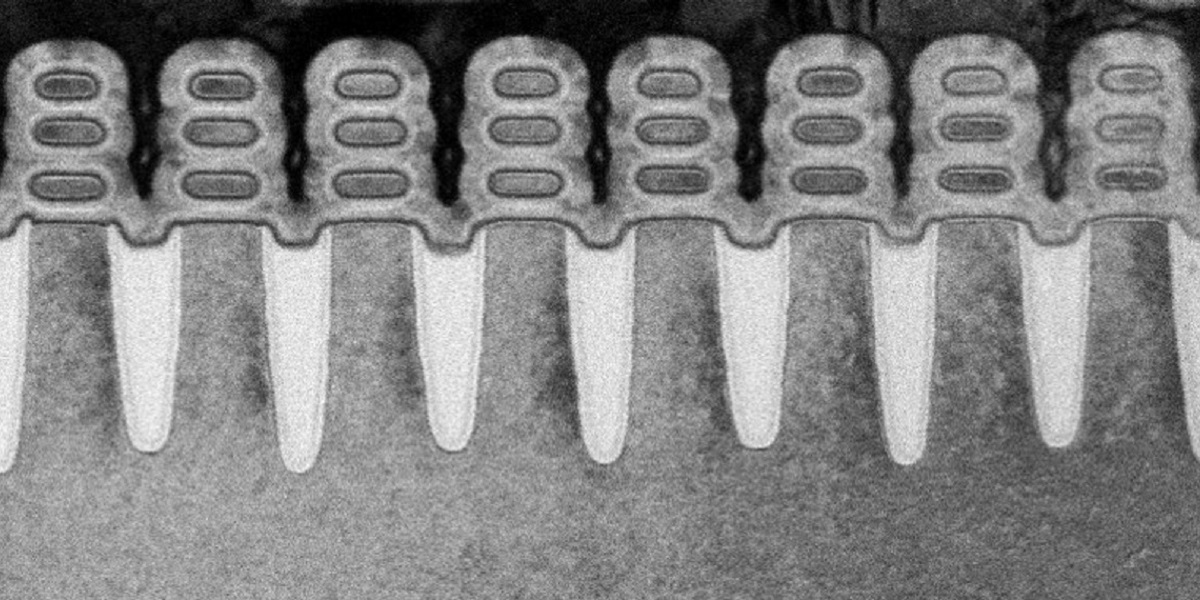
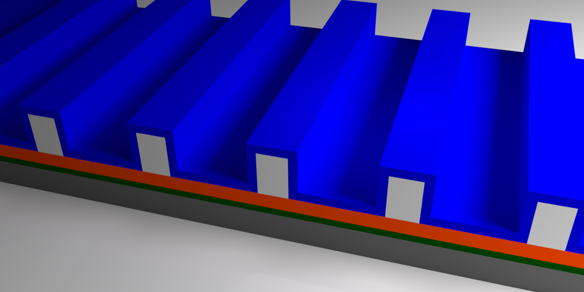
A few weeks ago, the big news was that the research alliance of IBM, Global Foundries and Samsung unveiled the world’s first 5 nm chip as we could all read everywhere over the internet [1]. Most notable was however the fact that they reported the use of horizontal gate-all-around field-effect-transistors (GAA-FETs) in which they actually … Read more

2nd Area-selective deposition workshop (ASD 2017)
– Flashback

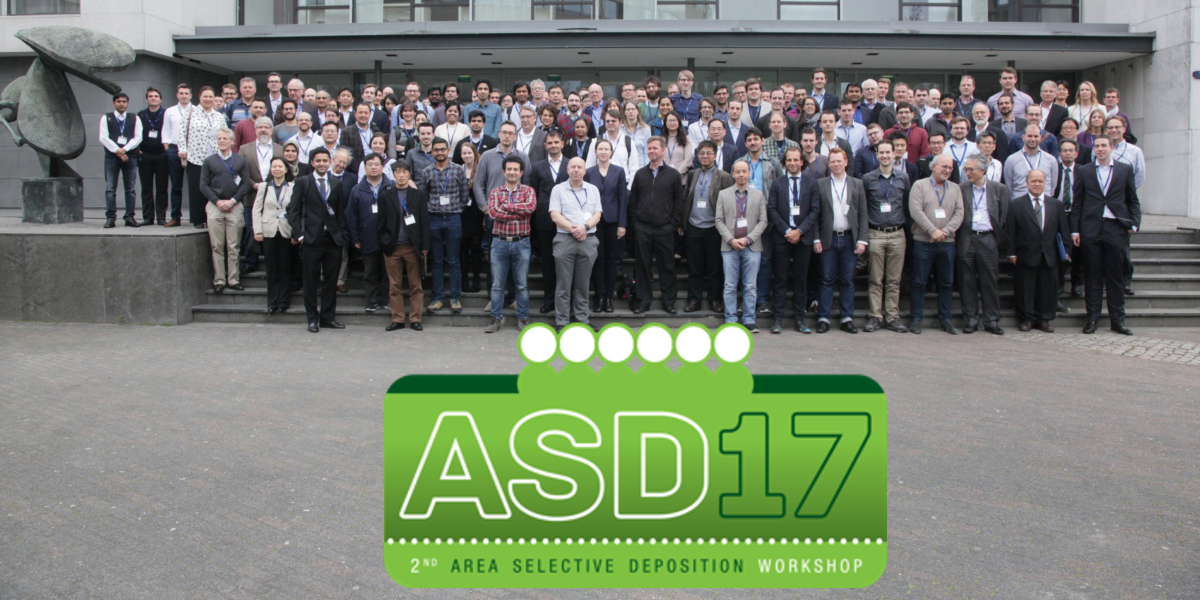
On April 20-21, the 2nd Area Selective Deposition workshop (ASD 2017) took place in Eindhoven.  Here we give a brief flashback of the workshop and include several photographs of the meeting, including a group photo of the participants. The workshop started on Thursday evening with a welcome reception. This reception took place on the campus … Read more

ALD-enabled nanopatterning: area-selective ALD by area-activation
– Reflecting on ASD 2016 with the ASD 2017 workshop approaching

The 2nd Area Selective Deposition workshop (ASD 2017, link) is approaching quickly now. The workshop will take place in Eindhoven on April 21 and my colleague Adrie Mackus is the main organizer. With the upcoming workshop in mind, I thought it would also be good to briefly reflect on the 1st ASD workshop at imec, … Read more

PECVD of amorphous silicon for lithium ion batteries
– How my PhD might be applied in industry

Recently I did an interesting discovery: the work that I did during my PhD (1996 – 2000) might be at the basis of a radical new technology to produce anodes of Li-ion batteries, anodes based on silicon nanowires instead of graphite. The Dutch branch of the company Meyer-Burger (Eindhoven) has sold a large tool to … Read more

X