
At the end of June (June 22–25, 2025), the ALD/ALE 2025 conference took place in Jeju, South Korea. The conference combines the International Conference on Atomic Layer Deposition (25th edition this year) with the Atomic Layer Etching Workshop (12th edition). Last year we celebrated the 50th anniversary of ALD in Helsinki, and I wrote a blog post about it. This year, I want to highlight ALE — and hence it is the focus of this blog post. One major ALE highlight was the plenary presentation by Dr. Chanmin Lee from Samsung, where it was revealed that 12 ALE processes are already in production across logic, DRAM, and 3D NAND manufacturing. This marks an important milestone for ALE, demonstrating that the technique is moving from research into high-volume manufacturing. We’ll come back to this later in this post.
This occasion also provides the perfect moment to look back at the origins and development of ALE. Just as we did last year for ALD’s 50th anniversary, we now share some significant updates to the historical timeline and the periodic table of ALE. But first, we start with a brand-new animation illustrating the two fundamental “flavors” of ALE.
Two Flavors of ALE
Before diving into the history, it is important to recognize that ALE exists in two distinct forms:
- Anisotropic ALE (plasma-based), where material removal is directional.
- Isotropic ALE (thermal or plasma-based), where material is etched uniformly in all directions.
To make this distinction clear, we created a new animation contrasting RIE and ALE. RIE (reactive ion etching) is well known in the etch community, with anisotropic processes (often desired for etching trenches, holes, vias, etc.) and isotropic processes (often undesired but very valuable for certain applications). The animation also shows isotropic and anisotropic ALE.
For anisotropic ALE, the animation illustrates how it can be used to remove the final part of material in a trench with a very soft and selective landing on the underlying layer — reflecting that ALE is generally too slow for etching an entire trench. For isotropic ALE, it shows how one material in a multilayer stack can be etched laterally, highlighting selectivity as a key consideration of etch process development (both to mask materials and the surrounding non-etch layers). This “indent etch” is essential in nanosheet gate-all-around FETs and in 3D NAND — something instantly recognizable to skilled practitioners.
Overall, this visual highlights how ALE — through its self-limiting nature — differs from conventional plasma etching and why it is becoming increasingly important for advanced nanomanufacturing.

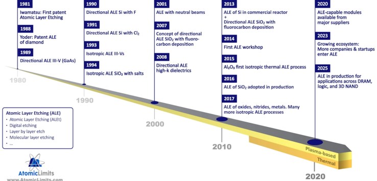
Updated ALE Timeline and Periodic Table
Last year we updated the ALD timeline to mark its 50th anniversary after Tuomo Suntola’s 1974 patent. We had previously presented an ALE timeline, but this timeline now requires an update. The new version highlights recent developments, in particular the fact that ALE-capable modules are now available from all major etch equipment suppliers and that the ALE ecosystem has been growing significantly.
A very significant update is historical. Researchers from AlixLabs discovered that the first ALE patent was not Yoder’s (1988), but an earlier patent by Iwamatsu (Seiko) filed in 1981. This correction has been highlighted recently at various places, a LinkedIn post by AlixLabs, a presentation at the ECS fall meeting in 2024 and a presentation at the ALE Workshop in Jeju where Fred Roozeboom gave a talk entitled The Invention of Atomic Layer Etching: on the Conception of Cycled Exposures of Silicon to Halogens and Pulses of Heat, Ions, and More, by Seiichi Iwamatsu.
Correcting this record provides a more complete view of how ALE concepts developed in parallel with ALD during the 1980s. As with ALD, maintaining an accurate history helps the community appreciate the continuity of ideas and the progression from early concepts to present-day applications.

Also in the animated periodic table, the 1981 origin is reflected. More importantly, the table now shows the growing number of ALE processes reported in the literature for different materials (both anisotropic and isotropic). The latest overview can be found in the ALE database on this blog. Please continue contributing by adding your own new ALE processes or those from the literature not yet captured. The ALE and ALD databases rely on crowdsourcing, so community input is essential.
ALE in Production – Insights from the Samsung Plenary
Returning to Jeju, one of the most impactful conference moments was the plenary talk by Dr. Chanmin Lee from Samsung. At the end of his insightful presentation, he disclosed that several more ALE processes have been implemented in high-volume manufacturing since their last report. Whereas three ALE processes were reported in DRAM at ALD/ALE 2024 (Helsinki), Samsung now reports 12 processes spanning DRAM, logic, and flash (3D NAND).
Below is the slide he used to illustrate this. It differentiates between ALE applications in logic, DRAM, and flash, and also distinguishes between anisotropic and isotropic processes, as well as between thermal and plasma ALE. Interestingly, the slide overlays Samsung’s new data onto a figure created by our PhD student Nick Chittock (now graduated and working for Oxford Instruments) for his award-winning ALD/ALE 2020 presentation. This presentation and the image can be found back in a previous blog post. Seeing Samsung build on this earlier work underlines how ideas in the community continue to evolve collectively.
We were pleased to see this connection, and I decided to recreate the figure with Samsung’s new data for clarity (see below).


Conclusion
Among many other things, the ALD/ALE 2025 conference in Jeju highlighted both the growing maturity of ALE and the importance of maintaining a clear view of its origins and evolution — much as has been done for ALD. With a corrected historical timeline, an updated periodic table, and new educational animations, we hope this blog post contributes to that effort.
ALE has now firmly established itself on the stage of atomic-scale processing in production. Together with ALD and ASD (area-selective deposition — on which there will also be news to share soon), it forms a a powerful toolkit driving the future of logic, memory, and beyond, though significant challenges remain to be addressed. As always, we welcome your feedback on these updates and look forward to seeing how atomic-scale processing methods continue to evolve in the years ahead.


Leave a Reply